Return to previous page Return to menu Go to next page

3.2 VRAM bank division

VDP2 can access four banks of VRAM-A0, VRAM-A1, VRAM-B0, and VRAM-B1 simultaneously by dividing VRAM-A and VRAM-B into two. As a result, more image data can be obtained at one time than when it is not divided into two, and the number of scroll screens that can be displayed at the same time can be increased, or a screen with a large number of colors can be displayed. However, there are restrictions on the VRAM read / write access specification by the CPU during the display period. Therefore, if you want to perform many read / write accesses by the CPU during the display period, you can perform efficient access by dividing the VRAM into two in normal cases and dividing it into two in normal cases.

■ RAM control register

The RAM control register specifies the VRAM bank division, the purpose of use of the rotary scroll screen VRAM, and the color RAM mode. This is a 16-bit readable / writable register located at 18000EH. The value is cleared to 0 after power-on or reset, so be sure to set it.

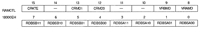
Color RAM coefficient table bit : Color RAM coefficient table enable bit (CRKTE), bit 15

Refer to “ 6.4 Coefficient Table Control ”.

Color RAM mode bits : Color RAM mode bits (CRMD1, CRMD0), bits 13, 12
Please refer to “ 3.4 Color RAM mode ”.

* When the CRKTE bit is set to 1, set the color RAM mode to mode 1. At that time, the second half of the color RAM (100800H to 100FFFH) is used for coefficient table data, so color data cannot be stored.

VRAM mode bit : VRAM mode bit (VRBMD, VRAMD)
Controls bank division of VRAM.

VRAMD
18000EH
 bit 8 
 for VRAM-A 
 VRBMD 
 18000EH 
 bit 9 
 for VRAM-B 


Return to previous page Return to menu Go to next page